J. Lu, Peking University and J. Ye, University of Groningen and I. Leermakers, N. Hussey, U. Zeitler, HFML-Nijmegen.
Compared with three-dimensional superconductors, atomically thin superconductors are expected to be easier to engineer for electronic applications. In this project, researchers from University of Groningen (Netherlands) together with colleagues from HFML and Hong Kong have used field-effect gating to trace out a ‘dome-shaped’ superconducting phase in a monolayer of the semiconducting transition-metal dichalcogenide, WS2. The remarkable doping range allows access to a cascade of electronic phases from a band insulator, a superconductor, to a reentrant insulator at high doping. The large spin-orbit coupling of ∼30 meV makes WS2 arguably the most strongly protected superconducting state against external magnetic field. The wide tunability revealed by spanning over a complete superconducting dome paves the way for the integration of monolayer superconductors to functional electronic devices exploiting the field-effect control of quantum phases. In the initial state with very few carriers, WS2 behaves as an insulator. The electric field adds carriers to this normal band insulator which increases the conductivity. At low enough temperatures, a superconducting state can then be realized. In the superconducting phase itself, the temperature at which superconductivity occurs first goes up with the increase of electric field, but then goes down again (Figure 1). This kind of dome-shaped curve was observed in many superconductors over several decades. Especially, this is one of the hallmarks of hightemperature superconductors, for which many mysteries remain unexplained. The superconductivity itself is exceptional in that it is robust to an intense magnetic field applied parallel to the monolayer plane. As shown in Figure 2, a field of 35 T only suppresses the superconductivity by 0.1 K. Even more surprising, however, was that as the electric field increases even further, the system goes from superconductor to insulator again, albeit a different kind of insulator. The authors suggest that the charge carriers in the material eventually become localized by the high electric field. Thus, they can no longer move through the material and it becomes an insulator. This is somewhat counter intuitive since higher gating typically means more carriers and hence improved metallicity. This discovery could pave the way for the rational design of two-dimensional superconducting devices that function at relatively high temperatures.
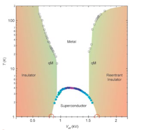
Figure1: Phase diagram of monolayer WS2. Superconducting
critical temperatures Tc are plotted (solid circles) as a function of
the effective back gate. Quasi-metal (qM) regime is bounded by
metal–insulator crossover temperature (empty squares).
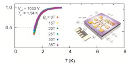
Figure 2: Ising pairing over the entire superconducting dome. (Left) Resistivity curves as a function of temperature at different magnetic field strengths up to 35 T. (Right) Schematic of measurement set-up with both ion liquid VTG and solid back gates VBG.
Full superconducting dome of strong Ising
protection in gated monolayer WS2, J. Lu,
O. Zheliuk, Q. Chen, I. Leermakers, N. E. Hussey, U. Zeitler, and
J. Ye, Proceedings of the National Academy of Sciences 115,
3551 (2018).

Leave A Comment
You must be logged in to post a comment.