Walter Escoffier, Michel Goiran, Mathieu Pierre, LNCMI Toulouse, and Oleg Makarovsky, University of Nottingham, UK.
Perovskite/graphene field effect transistors (FETs) have garnered substantial attention owing to their unique optical properties and potential for applications in electronics and optoelectronics, including ultra-sensitive photon detectors and FETs for metrology. The charge-transfer processes at the perovskite-graphene interface control the performance of these devices. However, a comprehensive understanding is still lacking especially in the presence of electric and magnetic fields. In this study, we explore the charge transfer in heterostructures of stable all inorganic CsPbX3 perovskite nanocrystals integrated with high-quality chemical vapor deposition (CVD)-grown graphene on SiO2 /Si substrates. Specifically, the performance of these devices is scrutinized under the influence of high electric fields (up to 3000 kVcm-1) and magnetic fields (up to 60 T) applied perpendicular to the graphene plane. We demonstrate the charge transfer to be markedly sensitive to the presence of electric and magnetic fields, and a slow (>100 s) charge dynamics. We also find a significant hysteresis in the charge transfer in magnetotransport experiments in constant (~0.005 Ts-1) and pulsed (~1000 Ts-1) magnetic fields. This aspect has not been widely explored in similar systems, and our work proposes a magnetic time constant (τmag) as a novel concept to explain and model the influence of magnetic fields on charge transfer in these heterostructures. We also observe quantum Hall-effect plateaus in the transverse magnetoresistance at low temperatures, a testament to the unique quantum phenomena exhibited by graphene in the presence of high magnetic fields. This, along with other observations, signifies the multifunctional potential of perovskite/graphene devices. Moreover, our study yields a two-capacitor model as a valuable tool for describing and understanding the complex charge distribution between graphene and perovskite nanocrystals, further elucidating the hysteresis effects in device behavior. By offering a deeper comprehension of the underlying physics, this work contributes to the integration of perovskite materials with graphene for applications in electronics and optoelectronics. High magnetic fields emerge as a crucial tool for probing the fundamental physics underpinning these systems.
a)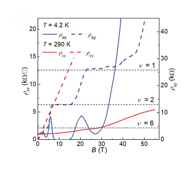 b)
b)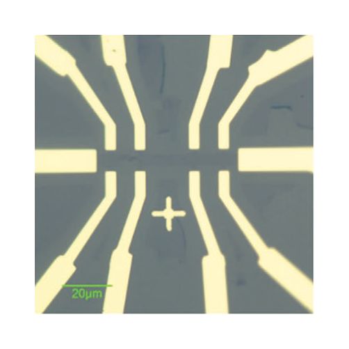
Figure: (a) Longitudinal (solid lines), ρxx, and transverse (dashed lines), ρxy, magnetoresistance at zero gate voltage, for T = 4.2 K (blue), and 290 K (red). Dashed black lines show positions of the quantum Hall-effect plateau with Landau index v = 1, 2, and 6. (b) Optical image of the graphene/CsPb(Br/Cl)3 Hall-bar device.
Magnetic and Electric Field Dependent Charge Transfer in Perovskite/Graphene Field Effect Transistors, N. D. Cottam, J. S. Austin, C. Zhang, A. Patanè, W. Escoffier, M. Goiran, M. Pierre, C. Coletti, V. Mišeikis, L. Turyanska, and O. Makarovsky, Adv. Electron. Mater. 9, 2200995 (2023).
https://onlinelibrary.wiley.com/doi/full/10.1002/aelm.202200995
Contact: walter.escoffier@lncmi.cnrs.fr, Oleg.Makarovsky@nottingham.ac.uk