Rosa Córdoba, ICMol and Uli Zeitler, HFML Nijmegen.
The fabrication and understanding of complex three-dimensional (3D) architectures on the nanoscale is one of the promising routes towards new schemes for a next generation of advanced electronic devices. This endeavor requires advanced new processing technologies, state-of-the-art structural and electronic characterization experiments, and cutting-edge theoretical models.
In this work, a team of researchers from Zaragoza, Paris, Madrid, Dresden, and Nijmegen has investigated the superconducting properties of 3D tungsten carbide nanohelices. They were fabricated by means of He+ focused-ion-beam (FIB) microscopy in combination with a precursor gas. The helices with pitches between 200 nm and 2.3 μm and diameters from 100 to 295 nm consist of nanowires as thin as 45 nm.
At temperatures below 7 K, these nanohelices display superconductivity with a large critical magnetic field (up to 15 T) depending on the direction of the field with respect to the helix axis. This suggest that the geometry of the helices and their orientation in a magnetic field play a significant role in the superconducting phase transition, which can be qualitatively explained using an approach for the properties of thin-film superconductors. In this respect, the results form an important starting point for a fully quantitative 3D modelling of superconducting nanohelices with dimensions comparable to or smaller than the superconducting penetration depth.
Eventually, as a more general perspective, the peculiar superconducting properties of novel nanostructures may then pave the way towards promising new device applications, such as sensors, energystorage elements, and nano-antennas.
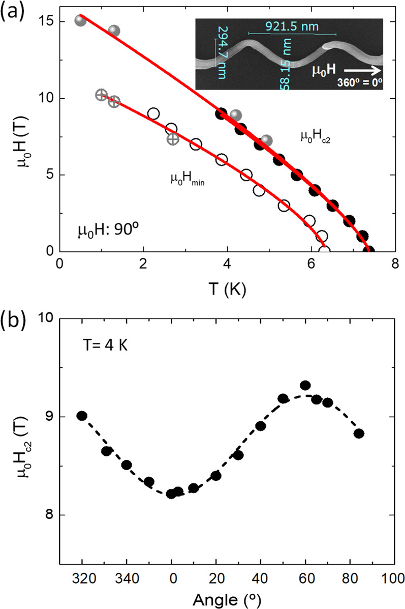
Figure: (a) Temperature dependence of the critical field of a tungsten-carbide nanohelix in a perpendicular magnetic field. The values for Hc2 and Hmin are determined from R vs. T and R vs. B sweeps as the points where the resistance reaches 90 % and 10 % of the normal-state resistance, respectively. The inset shows a scanning-electron micrograph of the structure. (b) Dependence of Hc2 on the angle between the helix axis and the applied magnetic field at 4 K, see inset in (a).
Three-Dimensional Superconducting Nanohelices Grown by He+-Focused-Ion-Beam Direct Writing, R. Córdoba, D. Mailly, R. O. Rezaev, E. I. Smirnova, O. G. Schmidt, V. M. Fomin, U. Zeitler, I. Guillamón, H. Suderow, and J. M. De Teresa, Nano Lett. 19, 8597 (2019).
DOI: https://www.ncbi.nlm.nih.gov/pubmed/31730351
Contact: uli.zeitler@ru.nl rosa.cordoba@uv.es